
Posted:9/26/2013 10:26PM
The Development of a VLSI Process to Create a Solar Cell
Mike Mclain discusses his personal experiences working inside a clean-room to create a VLSI solar cell process.
Posted:9/26/2013 10:26PM
Mike Mclain discusses his personal experiences working inside a clean-room to create a VLSI solar cell process.
Before I begin, allow me to provide a disclaimer and some brief background surrounding the content presented within this article.
Firstly, I want to make it very clear that this article is not going to discuss every process required to create a functional solar cell from start to finish (as the title might suggest) but rather will only discuss a few selective VLSI (very-large-scale integration) process steps that could be utilized in the development of a solar cell.
Secondly, while I do have a tendency to write my online articles from an academic perspective (as I generally enjoy providing information in great methodological/technical detail) thus such articles are typically fortified by the inclusion of a number of academic citations. Noting that such tendencies predominately arise when I am writing about a topic that is related to my personal research/interest. However, I want to make it understood that this article has not formally withstood the rigors imposed by an academic peer review and I think it is important to bluntly state such attributes upfront to avoid possible confusion.
Likewise, with this being stated, such sentiments do not inherently imply that the information provided here is either inaccurate or incorrect. In fact, I would argue that this particular article is very close to being (if it is not already) IEEE southeast conference worthy. Yet, I want to make you (the reader) aware that this article was written to convey my personal experiences/thoughts concerning the development of a VLSI process (as opposed to academic submission).
Thirdly, allow me to also formally state that I do not consider myself to be an expert within this particular research area (in the sense of academic specialization). While I do personally know and have had the honor of working under many professionals who are truly academic experts in this subject, I am also aware that they could metaphorically fly circles around me when it comes to total VLSI processing experience. Therefore, once again, allow me to state that the objective of this article was not to promote myself as an expert but rather to provide you (the reader) with insight into what working within this particular research area is like.
Fourthly, I would like to acknowledge my VLSI professor (Dr. Steven Bobbio) for his support in the acquisition of funding for this VLSI design project. Likewise, I would also like to acknowledge my colleague (Terence Goveas) who worked with me in the clean-room for countless hours to make this project possible.
Lastly, to provide some background information about this project, the results presented (within this article) are the product of a semester long class project (on the topic of Advanced VLSI processing) regarding how to develop (from scratch) a VLSI process that could be fabricated inside a mid-level clean-room (like the clean-room available at UNC Charlotte). Noting that a mid-level clean-room is not necessarily going to have the latest and greatest fabrication technologies like a billion dollar ULIS (ultra large-scale integration) machine nor is it going to be the best environment for the creation of sub-micron structures.
While such stipulations might be a letdown to a demanding reader (you have my apologies), I will offer the concession (in my defense) that in order for humanity to make some components commercially viable (like solar cells) the development of new and cheap processes are essential in achieving this goal. Hence why i argue that the development of such "lower-tech" processes (so long as such processes yield similar technical results even at a slightly lower quality than the original) are just as profound (if not more so) than creating a new and more exciting/expensive high-end process with few improvements.
To begin, (as it might be expected within any graduate level VLSI design class) the first week of the class was dedicated to tossing around potential ideas of processes that could be developed/fabricated within the class as a semester long project. Likewise, since the objective of this class was to learn advanced VLSI design (noting that the best way to acquire such knowledge is through doing rather than simply reading something from a book) it was very important that we selected an appropriate research project since this project would defined the problems encountered and the processing steps utilized.
Additionally, it should also be noted that VLSI processes (unlike other traditional electrical engineering subjects) does require more than the simple application of a design methodology (as there is no generic catchall recipe book) and while i will say that it is possible to create a device using only a well-defined recipe; however, I have observed that having a good visual intuition and an almost artistic preference (which is oftentimes unbounded by the burden of rigid methodology) is extremely beneficial in achieving such tasks. Noting that i have witnessed very smart and logically driven engineers struggle in VLSI design because they lacked "the artistic vision" of being able to intuitively visualize a structure and the steps required to make that structure a reality.
Thus, after spending time examining a number of different VLSI processing ideas (noting that solar cells were a hot topic throughout political discussions) we decided that creating a solar cell VLSI process from scratch would be a good research topic. Additionally, we also accepted the fact (at our professor's apprehension) that the lengthy and experimental nature of VLSI process development would probably make the odds of actually creating a functioning solar cell in one semester from scratch unlikely. Nevertheless, since the goal of the class was to learn processes (rather than build a fully functional device) this risk was acceptable and we decided to research this topic in further detail.
Likewise, after selecting this research topic (along with accepting that none of us was an expert in either solar cell technology or solar cell processes) it was decided that some background research should be done prior to trying to create a new VLSI process. Now, while I will not bore you with all the mundane details of this background investigation, I will provide you with a few fundamental facts just to cure my current nostalgia on the subject.
To begin, allow me to point out that a solar cell is (for all intents and purposes) an active electrical component that, upon interacting with light (assuming that all power production prerequisites are satisfied), will produce an electrical current at some defined (generally low) voltage. Noting that I used the term active component here to indicate that the device functions as a dependent electrical source (since the source is dependent upon the amount of light it receives). Likewise, it is important to recognize that the creation of an active component (at least from a VLSI processing prospective) is typically more resource intensive than creating a passive component (like a resistor or a capacitor) but is generally not as resource intensive as creating a complex integrated device (like a operational amplifier).
Conversely, it is also worth mentioning that the study of solar related electrical phenomena is not a new discovery. To demonstrate this fact, the first paper on the subject (at least to have received official scientific notarization and widespread publication) was written in French and titled "La lumiere, ses causes et ses effets" or Google Translated as (Light, its causes and effects) by Alexandre Edmond Becquerel in 1867. Now, while I would love to find an official English translation of this paper (but alas sometimes this is not possible with documents this old); however, Google's Language Translator can be utilized to gain some insight into the nature of Becquerel's work.
| # | Original | Translated |
|---|---|---|
| 01 | Cet ouvrage n'est pas un traite d'optique, car on n'y expose | This book is not a treatise on optics, because we are not exposed |
| 02 | aucun des principes generaux relatifs a la propagation de la | no general principles relating to the spread of |
| 03 | lu-miere ainsi qu'aux lois de la reflexion, de la refraction, de la | read-Miere and the laws of reflection, refraction, |
| 04 | diffraction , de la polarisation , etc... ; il ne comprend que | diffraction, polarization, etc.... , It includes only |
| 05 | quelques-unes des questions qui font ordinairement partie des | some of the issues that are usually part of |
| 06 | traites de physique et il renferme specialement , comme son | treatises on physics and contains especially as its |
| 07 | titre l'indique, l'expose des principaux faits concernant la | title indicates, the presentation of the main facts about |
| 08 | production de la lumiere ainsi que l'influence que les rayons | production of light and the influence that the rays |
| 09 | lumineux exercent sur les corps. | light exercise on the body. |
| 10 | Cet ouvrage, en outre, est purement experimental, et le petit | This book, moreover, is purely experimental, and the small |
| 11 | nombre de considerations theoriques qu'on y trouve ont ete | number of theoretical considerations found there were |
| 12 | jugees necessaires pour reunir et expliquer les faits. L'on a | deemed necessary to meet and explain the facts. It was |
| 13 | admis que le mouvement vibratoire de la matiere est cause | recognized that the vibratory motion of the material is due |
| 14 | des phenomenes lumineux et que la transmission de la | luminous phenomena and the transmission of the |
| 15 | lumiere a lieu , a distance , par l'intermediaire d'un milieu | light occurs at a distance, via a medium |
| 16 | ethere qui penetre tous tes corps; l'on a donc admis | entering all your ethereal body is therefore admitted |
| 17 | l'hypo these des ondulations, cette hypothese facilitant les | hypo thesis ripples, this assumption facilitates |
| 18 | explications que l'on peut donner et rendant compte de tous les effets | explanations can be given and reporting of all adverse |
| 19 | qui ont ete observes jusqu'ici. | that have been observed so far. |
Now, from this excerpt we can clearly see (at least based upon the translated text provided above) that (on line 10) Becquere says "... This book, moreover, is purely experimental ..." which implies that this particular publication was based mostly upon empirical information (likely observed while performing experiments in the laboratory). Similarly, based upon the translated text (found on lines 11 through 15) in which Becquere says "... It was recognized that the vibratory motion of the material is due [to] luminous phenomena and the transmission of the light occurs at a distance..." we are also able to recognize that Becquere (within the passage above) is alluding to observing solar related electrical phenomena that is (in contemporary times) referred to as photo-voltaic phenomena.
Now, while I personally did not translate and read every passage of Becquere's publication, I did discover that Becquere did make an interesting comment within the excerpts i did translate.
| # | Original | Translated |
|---|---|---|
| 01 | puis le commencement du quinzieme siecle jusqu'au milieu de | then the beginning of the fifteenth century until the middle of |
| 02 | celui-ci, epoque a laquelle ces phenomenes ont recu de grands | it, when these phenomena have received great |
| 03 | developpements. | developments. |
Likewise, from this excerpt (based upon the translations found on lines 1 through 3) Becquere states that "... beginning ... [with] ... the fifteenth century [starting at 1400] until the middle of [the] fifteenth century [ending around 1450] was a time in which the study of such phenomena ..." (assuming Becquere is referring to the study of optical phenomena) " ... [is when such] ... phenomena ... received great developments ...". Conversely, such passages (particularly within a scientific publication) generally implies the existence of other publicized documents, thus functions as a warning (particularly to an academic researcher) to perform a deeper background search on the subject.
Now, while I have observed that most modern scientifically driven people seldom possess an in-depth historical education on scientific events older than the twentieth century (as I personally did not possess such knowledge until I started doing background research for my dissertation). Yet, I was personally aware (from my research) that most of the formal scientific work surrounding electrical phenomena did begin with William Gilbert's "De Magnete" in the 1600s (in which Gilbert did attempt to summarize all the commonly known facts about electricity and magnetism that survived the Dark Ages). Furthermore, i also knew that some of the information Gilbert recorded had origin's dating back to Aristotle's time (but i begin to digress).
Nevertheless, I also knew that the fifteenth century (the time in which Becquere speaks of) would have been the tail end of the Dark Ages and around the time of the Renaissance so science (I would have figured during this period of time) would have been (to humorously put it) trying to preserve itself by remaining hidden in either some secret European archive or by roaming around in the back of a Middle Eastern caravan.
Yet, while I will admit that most people would just call the 1860's ancient history and talk about the next fundamental solar cell fact; however, I must confess that Becquere's little statement really did bother me and (in truth) it really should bother you since our beloved Wikipedia says Becquerel is the first person of interest on the solar cell time line while Becquere (in his own words) tells us that (at the very least) he had some type of influential source that dates back to the 1400s.
Now with this being said, the next logical question that arises (as a result) is: Was Becquerel trying to simply showboat his historical knowledge (by promoting this period of scientific history so the acute reader would reflect upon this period of time)? Or did something truly happen (during this period of time) related to his research that he thought should rightfully receive credit?
Either way I wanted to know the answer to this question, thus I started searching the internet in all of the obvious but academically inappropriate places (like Google and Wikipedia) just to try and obtain a rough idea of events that occurred during this period of time that were remotely related to optical phenomena.
Likewise, Wikipedia (in all its glory) responded to the fifteenth century inquiry with a rather lengthy list of possible historical events (surprisingly there were a few notable scientific figures like Nicolaus Copernicus on this list); However, such figures (like Copernicus) were born after the mid-fifteenth century so while it is possible that Becquere was paying homage to one of them (like Copernicus) but got the date wrong (contextually), I decided to research this attribute further.
Conversely, after refining my Google search to "15th century optics" Wikipedia (in return) led me to a page discussing the history of optics. Likewise, if earlier ancient works are ignored (Ante Christum through the early Renaissance) the names of both Johannes Kepler and Willebrord Snellius suddenly become possible candidates. Now, while Kepler (upon further review) is a sound possibility (albeit he is more frequently associated with Astrometry than optics) Snellius appears to have a stronger connection to the desired subject at hand (since he is associated with Ibn Sahls discovery of the law of refraction.
Nevertheless, while both possible candidates are significant contributors to the history of optics; however, both Kepler and Snellius were also born a century too late (as they were both born in the late 1500s) which makes it very unlikely that Becquere was referring to them within his work.
Thus, out of sheer frustration I decided to Google search the phrase "who invented solar energy" (the ultimate hail Mary search) and upon clicking the first link I found the answer provided was none other than Leonardo Da Vinci!
Now, because this source was far from academically "reputable" (as it claimed that Leonardo drew a sketch of a device that could harness solar energy) I decided to review Wikipedia again and discovered that Leonardo did (in fact) live around the period of time in which Becquere speaks (making Leonardo Da Vinci a viable candidate).
To investigate this notion further, i performed a Google Scholar search on Leonardo Da Vinci and discovered a primary source discussing this topic in great depth. Conversely, my investigation led me to the conclusion that Leonardo Da Vinci did (in fact) perform calculations on the power produced by solar rays reflected from a concave mirror (as he apparently held Archimedes and the idea of a solar mirror weapon in high regard), thus making him the likely person Becquere was referring to within his work.
Likewise, upon discovering this information (I will confess that) I swore a little under my breath since Leonardo Da Vinci's fascination with Archimedes is similar to Becquere's little paragraph that sent me off on this while tangent in the first place. Additionally, as I continued reading (the source i found) I also discovered that Leonardo Da Vinci also proposed that solar energy could be used for industrial purposes (noting that he created his own rendition of the Archimedes weapon as well).
Now, while the scholar inside me was compelled to dig into Archimedes' past and find the earliest historical documents regarding the usage of solar power; however, given the limited scope of this particular project I decided that I had more than enough historical information to quench my curiosity surrounding Becquere's statement.
Conversely, i also concluded that Becquere was probably paying homage to Leonardo Da Vinci in a rather cryptic manner (although i cannot rule out the possibility that Becquere might have been trying to include other "less notable" historical figures since perspective art was also popular in the fifteenth century and utilizes optical theory).
Nevertheless, while some might find this little historical tangent unnecessary; however, I personally believe that such information helps to convey the overall age of the subject and illustrates how science is a progressive process that continually builds upon previous work (typically through the modification of existing theory or through providing a solid intellectual framework to build a new theory upon).
Now that we have (hopefully) resolved the Becquere Code (yes this is my witty attempt to satirize the Da Vinci code), let us briefly discuss how solar cells function (at least from a theoretical perspective) with the caveat that the more gritty scientific attributes will not be discussed in substantial detail (although i do recommend that the curious reader find a scientific website about photovoltaic or PV effects to learn more information about the subject).
To begin, photovoltaic (or PV) effects are said to occur when light and a material (like doped silicon) interact with each other and electricity is produced (within the material) as a result. Conversely, while this definition is relatively straightforward to apply (as anyone can understand the concept that light hits a material and the material makes electricity as a result) it is "the how" and "the why" of the PV definition that is difficult to conceptually rationalize. Now, while nobody really knows "why" nature is the way it is (although books on the philosophy of science discusses this attribute in more detail); however, the question of "how" is a subject that science can predict (within a humans perceptive ability) with modeling very accurately.
Likewise, without diving very far into the depths of philosophical discussion, let us now focus solely upon "the why" rather than "the how" of PV theory. Conversely (in order to achieve this objective), we must first examine some basic PV fundamentals, and although I will not provide all the gory scientific details, I will (nevertheless) endeavor to explain this information in terms that a layman can understand for the sake of clarity.
To begin:
Now that some basic terms have been defined, allow me to roughly describe the basic premise behind how a simple p-n type solar cell operates. First, a solar cell is generally created by taking a semi-conductive base material (like Silicon) which (if left alone) is not electrically conductive (since Silicon's band gap energy is rather high so electrons cannot move around freely). Likewise, new chemical bonds (with other elements) are forced to occur within the silicon structure (or lattice) through a VLSI process called doping. Additionally, because orbitals (or bands) try to minimize energy and some chemical bonds yield more electrically conductive orbitals (or bands) than others do, different materials can be doped with the silicon to either promote or discourage electrical conduction (normally with the intent to permit the external control of electrical conduction via the application of an external voltage or current source).
While there are several methods (within VLSI) to dope Silicon and some of these methods involve propelling atoms (at a high velocity) into a Silicon lattice (like a metaphoric Sci-Fi mass driver); however, it is important to remember that the doping process is ultimately designed to change the electrical properties of a desired material (like a Silicon wafer). Likewise, when a p-type dopant (or an element that naturally tries to transition electrons from shared conduction orbitals into unshared orbitals in order to lower net energy) is implanted into a material (like Silicon), the p-type material makes the material give up electrons which (in turn) creates a reduction in the overall electrical conductivity of the doped materiel. Similarly, when a n-type dopant (or an element that naturally tries to transition electrons from unshared orbitals into shared orbitals in order to lower net energy) is implanted into a material, the n-type material gives the conduction orbitals (between the base material and the n-type material) its electrons which (in turn) increases the overall electrical conductivity of the doped material.
Conversely, both of these doping processes ionize the doped material (implying that, in the case of Silicon, the Silicon will possess an effective charge imbalance) and if two dissimilar doped materials are combined together (one slab next to another) they will create a p-n junction which has a boundary (between the two dissimilar doped materials) that tries to remove charge imbalances (created via ionization) in order to reach a non-conductive electrical state (or at least this state is non-conductive until an external energy source is applied correctly across the p-n junction). While the electrical properties of p-n (or diode) junctions are interesting, this particular attribute is not as important (within the scope of our discussion) as the p-n junction's ability to absorb photons (an act that can displace electrons within the p-n junction and result in the creation of electrical current). Likewise, it is this fundamental capability of a p-n junction (to convert photons into electrical current) that makes the development of a solar cell possible; however, because (in the case of Silicon based solar cells) not every photon is capable of being absorbed by a p-n junction (noting that the Physics explaining this phenomenon is very complex and is also a function of a utilized material's band gap energy) it is very difficult to create a p-n junction that is highly efficient in capturing all solar radiation (hence why solar cells are currently not very efficient).
Now, while there is more to this story than summarized above, I do believe that such descriptions are adequate enough to provide some basic insight into how a solar cell works and the type of background research that was required prior to proceeding into the design phase of the VLSI project. Likewise, once we knew enough about the fundamentals of solar cell processes to enter the design phase, we started throwing around ideas in order to create a new solar cell process. Conversely, (based upon the information we obtained) we decided to develop a solar cell process that would utilize small sub-micron fins to see if the p-n junction's rate of photonic absorption could be increased (or in other words we were trying to increase the number of photons that could be absorbed by the junction through the usage of process geometry, since such geometry, if designed correctly, can absorb more solar radiation).
While the creation of sub-micron structures might sound relatively straightforward in the VLSI processing world, keep in mind that we were attempting to make these structures in a mid-range cleanroom that predominantly utilized lithography methods that had a limited amount of overall optical resolution.

To elaborate on this attribute further, because the creation of a lithography mask with sub-micron size features is both a complex and expensive process (because we typically have to outsource the creation of these mask elsewhere) , we decided to recycle an existing lithography mask from a previous semesters VLSI oscillator project per Dr. Bobbio's suggestion (noting that if I knew whose VLSI project the oscillator mask was from I would have given them credit here). Likewise, upon acquisition of the oscillator lithography mask we started our VLSI process by spinning a thick layer of photoresist (I believe 100 microns or so in thickness) onto an n-doped Silicon wafer and then performed the required lithography steps needed to transfer the oscillator mask onto the wafer. Conversely, these steps included spinning on photoresist, heating the wafer up a bit to cure the photoresist, activating the photoresist with UV light to transfer the lithography mask to the wafer, and developing the photoresist mask with chemicals.
Next, a highly selective Silicon etch was done with a high aspect ratio plasma etcher and while I personally do not recall the exact gases that were used (within the plasma etcher) to perform the etch (I believe it was probably CF4 or SF6) the results obtained were examined using a scanning electron microscope (SEM) to determine if the process step was successful.
Likewise, upon examining the etched wafer using the SEM, one of the first problems we ran into (because of the small feature size of the oscillator mask), was an issue with the lithography UV exposure time. Now, while this might sound somewhat funny; however, (oddly enough) we had both over and under UV exposure on the same wafer and we (after some further research) believe this phenomenon occurred because the photoresist deposited (on to the wafer) was not being uniformly distributed during the spinning step of the process because of the photoresist thickness selected to ensure adequate coverage during the plasma etch step.
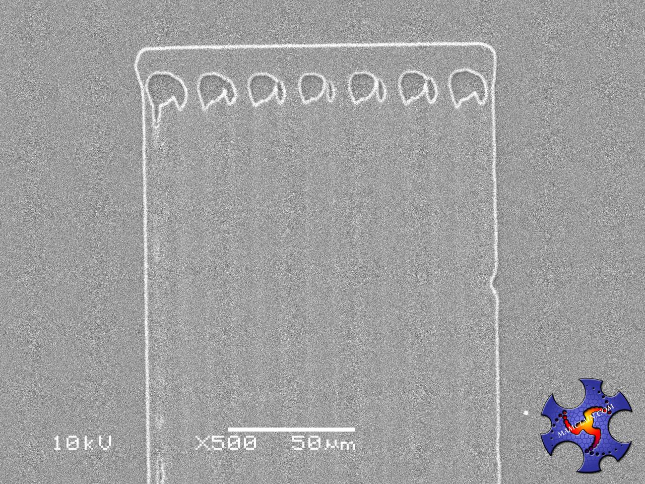

Fortunately, parts of the etched wafer also had good lithography and, in turn, we examined these areas at a higher resolution using the SEM to check the etch aspect ratio.


At this point we concluded that this part of the VLSI process was successful (at least for process development standards) and when we had to perform this step again (in order to make a batch of these wafers to move to the next process step) we tried to avoid exposure issues by being more careful during the lithography process.
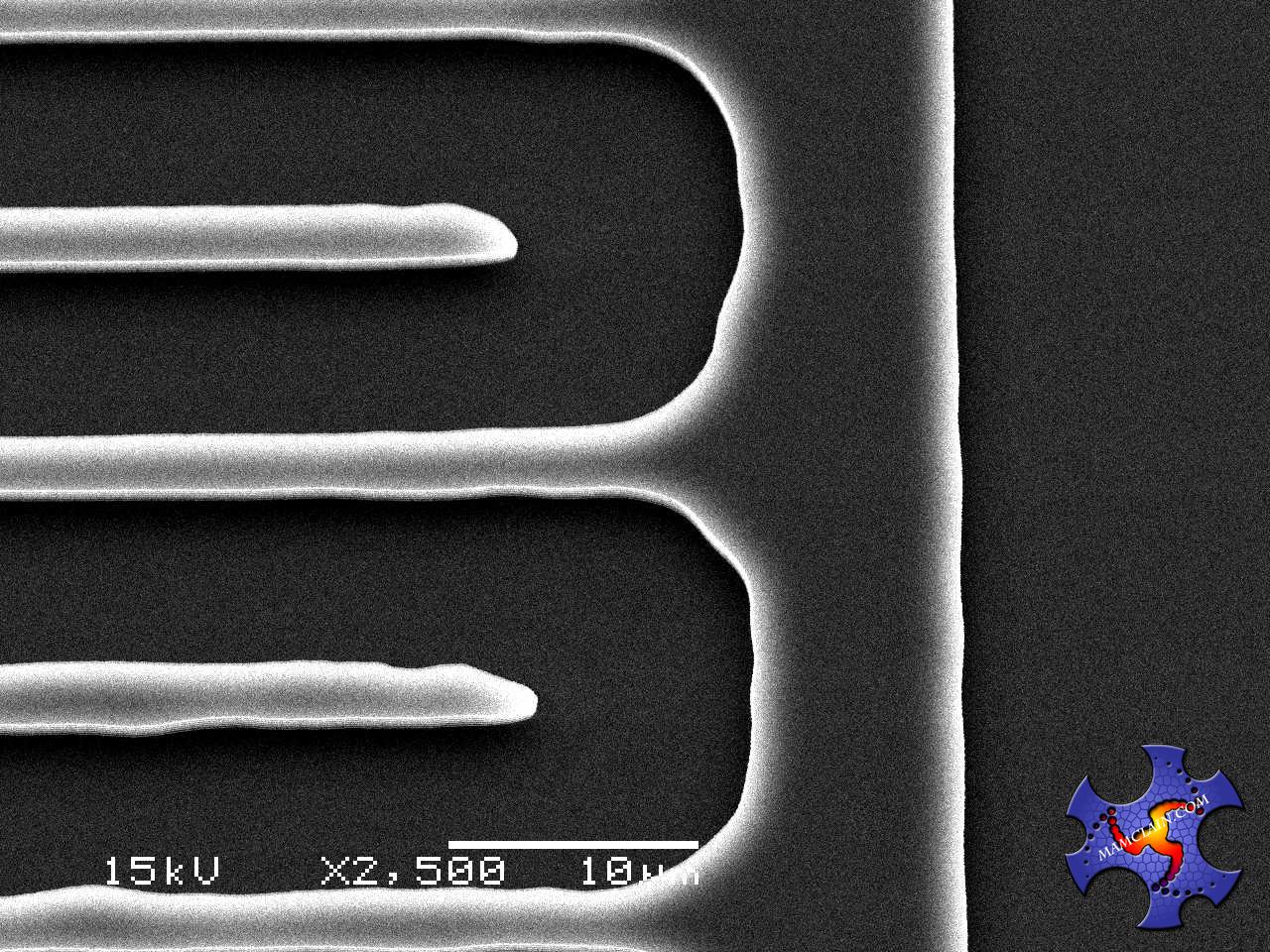
Next, we briefly did some simplistic post-process cleanup of the photoresist mask (I believe we utilized a quick dip in piranha etch to remove the photoresist). Afterwards, because we wanted to create sub-micron structures but the oscillator mask we were using had fins that were around five microns in size, we decided to oxidize the whole wafer with the goal of achieving a micron of sidewall oxidation that could be utilized as a sub-micron mask. This oxide mask (in turn) should allow us to achieve sub-micron features inside a clean room that is really not designed to produce such small structural features. Likewise, after the wafer was oxidized (via a stay in a 1000 centigrade oxidation furnace for a number of hours), it was observed using the SEM again to determine how much sidewall oxide remained on the wafer.

After the wafer was observed using the SEM, we decided to etch the oxide layer with a general plasma etcher (I believe using either the gas CF4 or SF6) and the results obtained were once again observed using the SEM.


Next, because the SEM indicated that a successful oxide spacer was created we decided (at least based upon the results we obtained) that we were ready to perform another high aspect ratio plasma etch. Likewise, after performing this etch and analyzing the results using a SEM, it became apparent that tragedy had struck (as the small sub-micron structure had shattered during the etching process)!
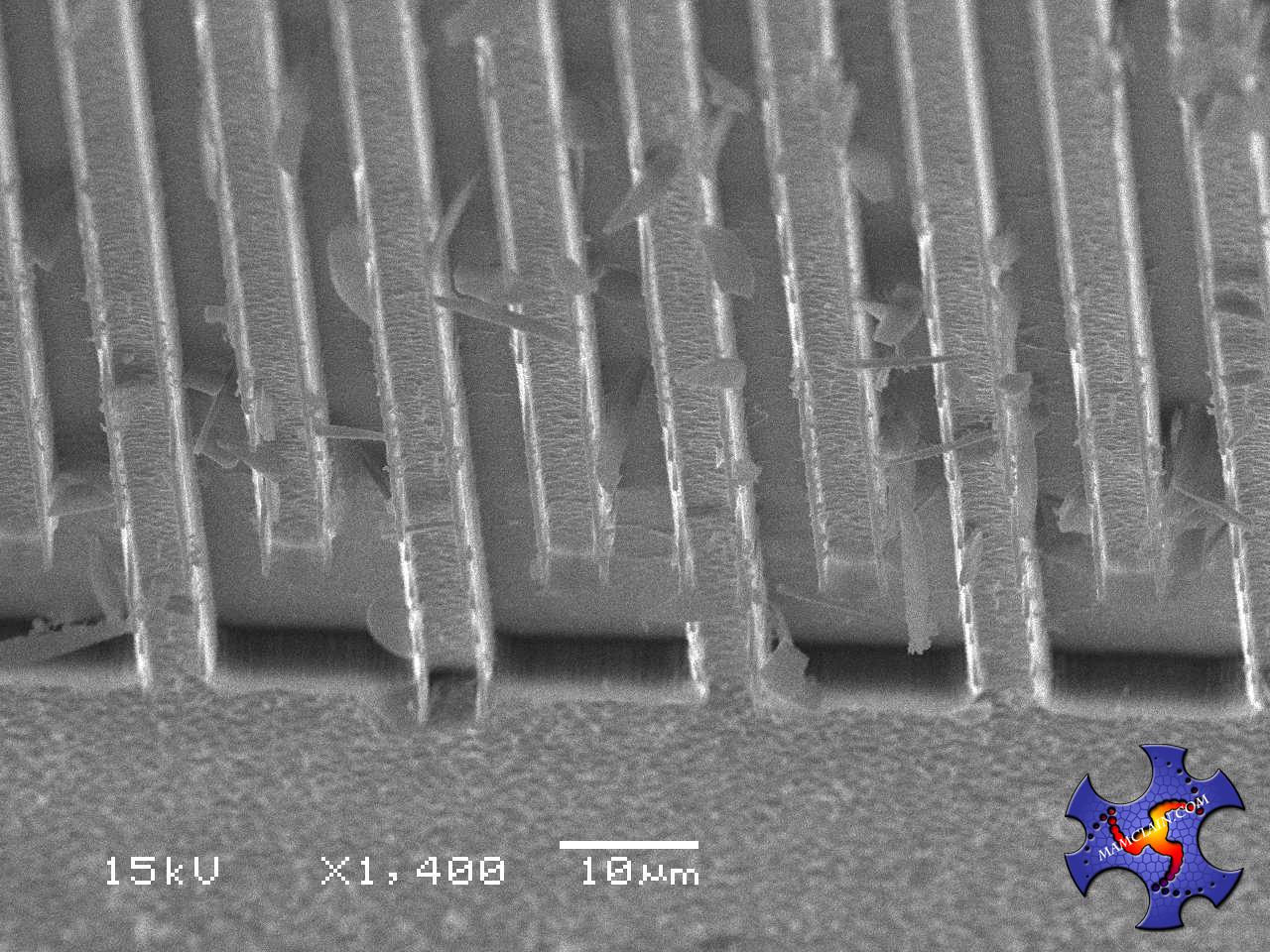
Sadly, around the time this tragedy occurred, the semester ended and our work on this project was concluded; however, (after examining the wafer) we believe that the sub-micron structure shattered because the tensile stress incurred (upon application of the oxide growth step) became greater than the masked structure could handle upon removal of the oxide spacer. Nevertheless, despite this bitter outcome, i found learning about VLSI processes to be a wonderful experience (noting that such bitter occurrences effectively articulate the inherent complexities associated with working within this particular research area).
At any rate, I hope you enjoyed reading this article!
By Mike Mclain